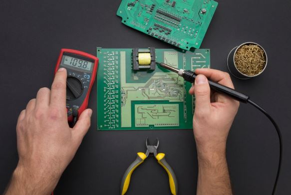
Not every PCB layout is a straightforward exercise in placing components and routing traces. High-speed digital designs with impedance-controlled differential pairs, dense HDI boards with 4000+ pin BGAs, rigid-flex assemblies with multiple bend zones, and RF circuits operating at microwave frequencies all require specialized design knowledge that many general-purpose layout houses do not possess. When your project pushes beyond standard complexity, finding the right PCB design company becomes one of the most important decisions in your development cycle.
Know When Your Project Exceeds In-House Capability
Many engineering teams have internal layout resources that handle routine two-layer and four-layer designs effectively. The need for an external design partner typically arises when a project involves one or more of the following:
- High-speed signal integrity requirements with controlled impedance traces, length matching, and differential pair routing
- HDI stack-ups with microvias, blind and buried vias, and fine-pitch BGA escape routing
- Rigid-flex or flex designs with bend-radius constraints, coverlay requirements, and stiffener placement
- RF or microwave circuits requiring specialized substrates like Rogers or Duroid and careful attention to transmission line geometry
- Schedule pressure that exceeds the bandwidth of your internal layout team
Recognizing these triggers early prevents the delays that result from an internal team struggling with unfamiliar technology or a design that requires multiple respins to get right.

What Separates a Qualified Design Partner from a General Layout House
An experienced PCB design company brings more than the ability to operate layout software. Evaluate prospective partners on these criteria:
- Designer certifications: CID+ (Certified Interconnect Designer Advanced) certification from IPC indicates that the designer has demonstrated proficiency in advanced layout techniques and understands IPC design standards.
- Tool proficiency: Your design partner should be proficient in the CAD platform that matches your workflow, whether that is Cadence Allegro, Siemens Xpedition, PADS, or Altium Designer. Ask about their experience with the specific tool your project requires.
- DFM integration: The best design partners do not simply produce a layout and hand it off. They run design-for-manufacturability analysis using tools like Valor NPI to identify fabrication and assembly issues before the board reaches the manufacturer.
- Signal integrity analysis: For high-speed designs, ask whether the partner performs impedance modeling, crosstalk analysis, and timing verification, or whether they rely on the customer to provide all constraints.
- Stack-up expertise: Complex multilayer boards require careful stack-up planning to balance impedance targets, material availability, cost, and fabrication feasibility. Your design partner should collaborate with you and the fabricator on stack-up definition, not treat it as an afterthought.
Why Design-to-Manufacturing Alignment Matters
A PCB design that looks correct in the CAD tool may still cause problems on the production floor. Insufficient solder paste apertures, test point placements that conflict with bed-of-nails fixtures, component footprints that do not match actual part dimensions, and copper features that violate the fabricator’s process limits are all issues that a design partner with manufacturing awareness will catch before fabrication.
This is where the distinction between a standalone layout house and a full-service partner connected to manufacturing becomes clear. Circuit board manufacturing companies that also provide design services maintain a continuous feedback loop between their layout team and their production floor. Design decisions are informed by real manufacturing data, not just CAD rules.
The Value of a Single Partner for Design and Assembly
When your design partner and your assembly partner are the same company, file handoff errors disappear. The designer who laid out your board can walk to the production floor and discuss a DFM concern with the assembly technician directly. Engineering changes propagate instantly without the delays and miscommunication that occur when design files must be exported, packaged, and transmitted to a separate organization.
For engineering teams with limited internal resources, this consolidation also means fewer vendors to manage, fewer purchase orders to process, and a single point of accountability for the entire project.

MJS Designs, Inc. is one of the most experienced and reliable PCB design company partners in the United States, with over 45 years of expertise in high-speed digital, RF, HDI, and rigid-flex layout. With CID+ certified designers, proficiency in Cadence Allegro, Siemens Xpedition, PADS, and Altium, and Valor DFM verification on every design, MJS Designs delivers the specialized capability that the best circuit board manufacturing companies are recognized for, all under one roof, from design through assembled and tested boards.